Search Archive
📌 Pinned

AVIC - N1 bypass w/Hi-res board scans..

By ballerinstaller · Apr 29, 2006in Hacks/Mods💬 108 posts👁️ 88,682 views
Page 1 of 5
Posted Apr 29, 2006 · 07:17 UTC#1
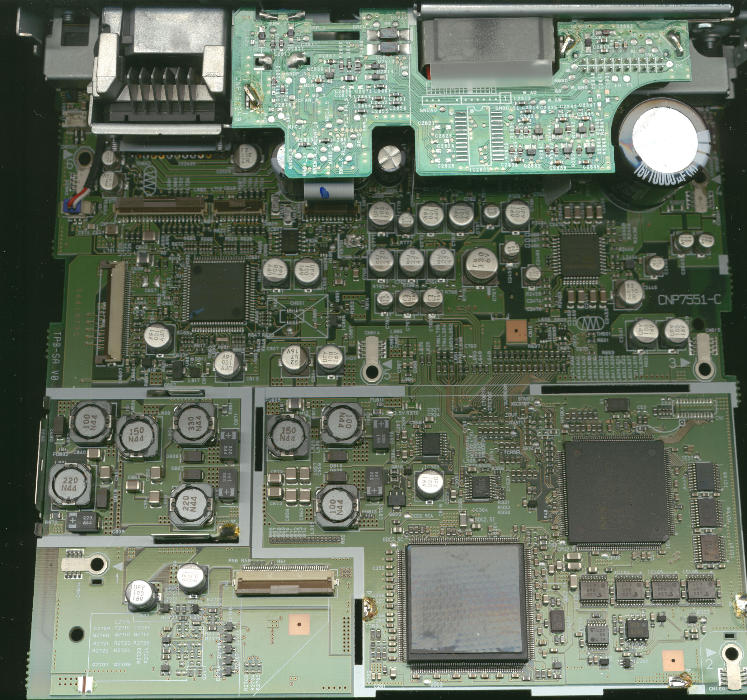
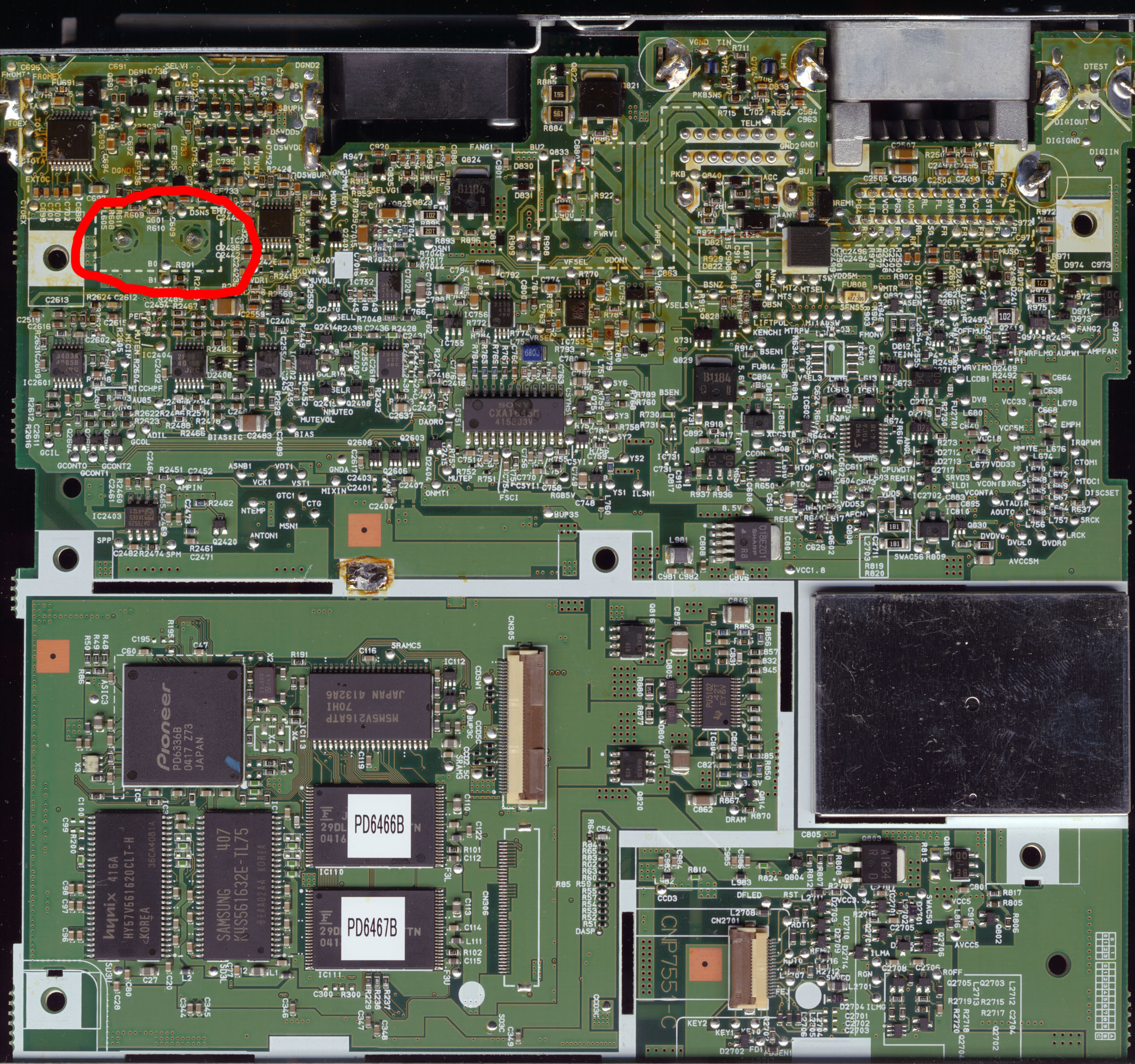
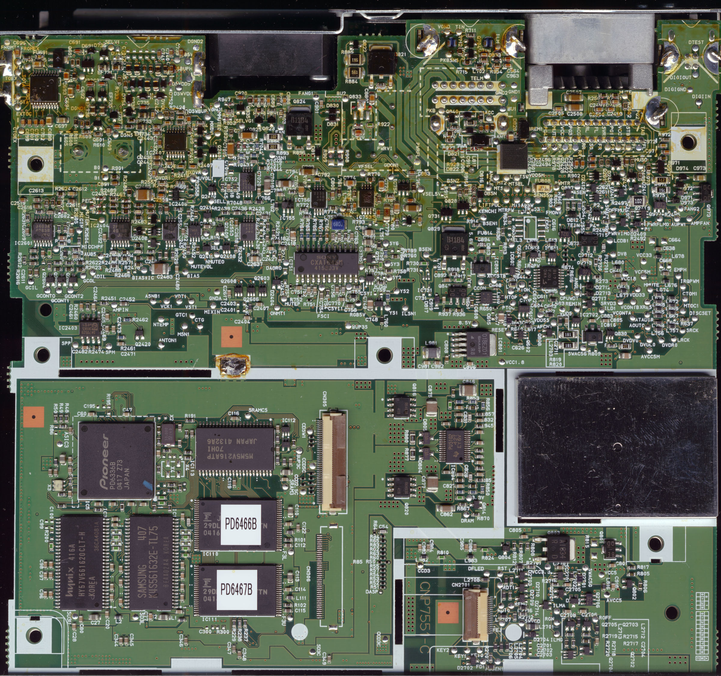
Here they are! So lets all line up to the starting point and get this race started to find the magic resistor on the N1 that bypasses the lockout that plague the 50mt and newer software releases....
Attached Files (2)
Bottom sidetiny.jpg
Bottom sidetiny.jpg
top sidetiny.jpg
top sidetiny.jpg
Posted Apr 29, 2006 · 13:58 UTC#2
wow, i wouldn't know where to even start to design a circuit board, that's just crazy.
Posted Apr 30, 2006 · 03:38 UTC#3
any chance to get a pic of the n2 or n3 board so i have something to compare with? i mainly need the part where r197 is located, front and back of that part. i deal with circuit boars all day long.
Posted Apr 30, 2006 · 04:09 UTC#4
Breadboarding that would be such a pain!
Posted May 05, 2006 · 17:40 UTC#5
Anyone got the answer for this yet?
Posted May 09, 2006 · 00:18 UTC#6
need pics of a n3 or n2 board to figure it out
Posted May 09, 2006 · 02:44 UTC#7
Get a CitcuitWriter and connect these. I do not have an n1 but this is in the same area as the n2 and n3
Attached Files (1)
bottom_sidetiny_214.jpg
Posted May 09, 2006 · 13:15 UTC#8
Are you sure? I thought it was somewhere else.
Posted May 09, 2006 · 15:39 UTC#9
Yea here is a photo of my n3 when i bypassed it. The n2 is is the same spot just dose not have a switch.
Attached Files (1)
avic-n_bypass.jpg
avic-n_bypass.jpg
Posted May 10, 2006 · 06:16 UTC#10
That is the power supply dolt! That will smoke the mains fuse.
Posted May 16, 2006 · 16:30 UTC#11
any hi res of a n2, n3??
Posted Jun 12, 2006 · 20:02 UTC#12
woo hoo...
Posted Jun 12, 2006 · 20:03 UTC#13
Could IMODEON mean Interlock Mode On???

HUM??
Posted Jun 14, 2006 · 02:17 UTC#14
I'm not trying to be sarcastic "guest", but where's the proof it worked for you?
Posted Jun 14, 2006 · 02:21 UTC#15
Sorry, didn't realize it didn't auto-log me in when I made the previous comment about showing proof. :oops:
Posted Jun 14, 2006 · 21:05 UTC#16
In my car.
A guy on e-bay does them all the time.
Trying to do the forum a favor, but let's face it, most of you couldn't get the thing apart without tearing the screens flex cable, breaking ribon cable sockets, and screwing up the motherboard with your 500W radioshack soldering gun.
Forget I even posted it!

MODERATOR, TAKE THE POST DOWN PLEASE.
Posted Jun 15, 2006 · 00:44 UTC#17
Anonymous said:
In my car.
A guy on e-bay does them all the time.
Trying to do the forum a favor, but let's face it, most of you couldn't get the thing apart without tearing the screens flex cable, breaking ribon cable sockets, and screwing up the motherboard with your 500W radioshack soldering gun.
Forget I even posted it!

MODERATOR, TAKE THE POST DOWN PLEASE.


I said I wasn't trying to be sarcastic. Just the fact that you were listed as "guest" made me question it, that's all. Anybody could pop in here unregistered, post what they claim is the fix resulting in someone trying it and frying an expensive piece of equipment. Believe me, if that is the solution, all of us will be eternally gratefull.
Posted Jun 15, 2006 · 15:22 UTC#18
Maybe I am trying to be Anonymous.

If you want go to ebay and buy a service manual for the N1, N2, and N3.
Look at the N3 and it will say to use the N2 manual along with the N3 manual for additions. One addition is the SWITCH. The N2 manual doesn't talk about R197 since it is not filled with a component. Why reference it if it never needs to be repaired. Since the N3 has a SWITCH it is referenced and shows you what it does.

The schematic where the switch goes is the same as the N2 and N1.
THE IMODEON is in the same location on all there.
THE R197 and S151 (switch) are routed from the underside (for acessability) to the A side of the main board. Since the N1 doesn't have either R197 or S151 you need to do it on the A/main side as noted in the picture.

AGAIN, the parts are small and MOST will damage their $300+ main board (CC Unit) trying to solder this small of components.

PAY SOMEONE TO DO IT that is competent. I don't want to be held acountable for anything!

If someone wants to prove it... Take your N2 or better yet N3 and take it apart. Test for continuity from the marked areas (same on all three) to the R197 or S151. You will see that it is the SAME.


Thanks MOD for keeping this forum Anonymous for the people who have knowledge and want to share without compromising anything. I guess unless you log IP's and have a court order to give them up. I SURE HOPE NOT!
Posted Jun 15, 2006 · 16:06 UTC#19
:oops: :oops: :oops: :oops: :oops: :oops: :oops: :oops: :oops: :oops: :oops: :oops: :oops: :oops: :oops: :oops: :oops: :oops: :oops:

I AM SORRY!!!
I DREW THE WRONG LOCATION.
PLEASE DON'T USE THE FIRST PICTURE WITH THE HACK. IT IS WRONG!!!

REPEAT:

DON'T USE THAT HACK! IT REFERENCES THE WRONG POINTS!

MOD/ADMIN - PLEASE REMOVE THE PICTURE WITH THE WRONG HACK.

:oops: :oops: :oops: :oops: :oops: :oops: :oops: :oops: :oops: :oops: :oops: :oops: :oops: :oops: :oops: :oops: :oops: :oops: :oops:
Posted Jun 15, 2006 · 17:56 UTC#20
I am waiting to post the correct picture of the hack once the mod deletes the wrong one so there is no confusion.
Posted Jun 15, 2006 · 21:12 UTC#21
Anonymous said:
I am waiting to post the correct picture of the hack once the mod deletes the wrong one so there is no confusion.


Can you post your picture without waiting? Right picture will not confuse people.
I send my unit for mod to VA and it should arrive soon. I’ll compare if this is same procedure. Also, how you find this out?
Posted Jun 16, 2006 · 11:56 UTC#22
..........
Posted Jun 16, 2006 · 15:55 UTC#23
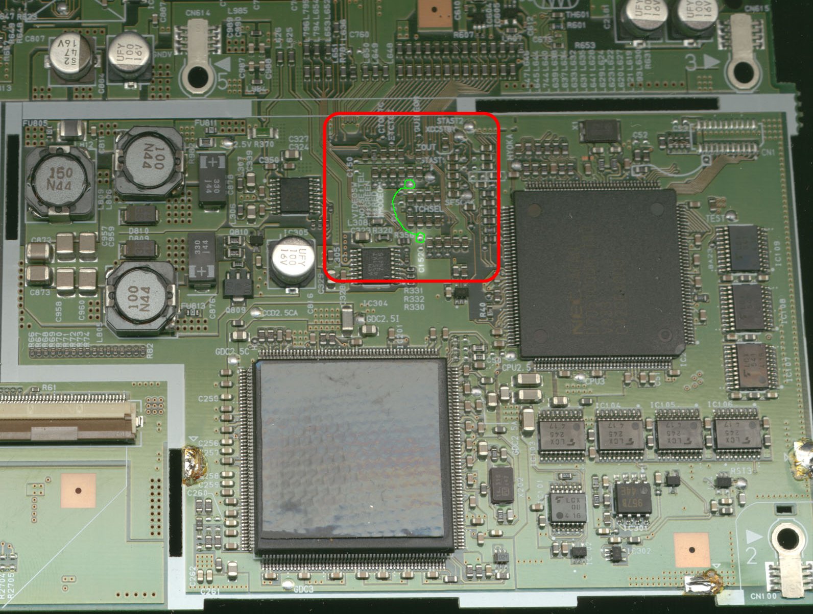
Here is the correct mod.

I was reading the schematics after the inital post and it started to not look correct and it wasn't. I was going from memory when I drew the first one.

The top connection is CORRECT in both picts. This doesn't change unless you want to go directly to the pin on the ASIC chip on the B side.

The bottom connection I incorrectly drew on the first post is not the correct line.

The line connects to many components near the one I am posting here in GREEN, but the point where I drew is an easy point to solder to.

You can tag more than a half a dozen spots that share the smae line even on the other side of the motherboard. The B side (other side) is where the ASIC chip (PD6336B) resides anyway, but it is easier to do the mod on the A side so you don't have to take the board out of the chassis OR un-solder the sheilding cover the chips that reside on the bottom.

SORRY for the error.
Attached Files (1)
avicn1_HACK.jpg
avicn1_HACK.jpg
Posted Jun 16, 2006 · 18:33 UTC#24
Sorry man... I also can't see what Guest is trying to show. What exactly was modded on the N1 picture? And a dumb noob question. Is this circuit board on the brain unit or the HU?

This work for the 60MT discs?
Posted Jun 16, 2006 · 18:37 UTC#25
My bad... I see the hack now. Still have the question about where this circuit board is located.

Thanks.
Page 1 of 5